Techniques for Setting up Peripherals via PIO and DMA
Published at – 14 min read – 2867 words
In Part 5 of our series, we focused our efforts on understanding how the firmware was structured. In doing so, we analyzed the folder with the system executables and delved into the various configuration files.
Before tackling the analysis of a device driver, we need to focus on some hardware aspects that will come in handy for this article. These aspects include the management of peripherals and input/output devices.
The Registers Associated with the Peripherals
Mouse, keyboard, webcam, and optical sensors all have something in common: they are all peripherals ― hardware devices that extend the functionality of a computer and interface with the real world. There are input peripherals (e.g., mouse, keyboard, sensors in general), output peripherals (e.g., keyboard), but also input/output peripherals (e.g., the network card).
Peripherals have always been difficult to manage because of the countless different configurations between manufacturers. How can we get the operating system and peripheral to talk to each other? Each peripheral has associated registers and a hardware controller that allow low-level commands to be issued to the peripheral. A hardware controller is an electronic interface that allows a device to be commanded (e.g., move a frame, configure the device’s mode), while a register is a very expensive, but also very fast and volatile memory that allows virtually instantaneous exchange of information.
Each device/peripheral consists of at least three registers:
- a register for data (data register) containing some information that the operating system needs to know (e.g., mouse position, keyboard character typed);
- a register for the status of the peripheral device (status register) that makes note as to whether it has been recently used, whether some sudden error has happened, etc.; and
- a register for the control (control register) that allows commands to be given to the device.
By accessing data from these registers, any device can be configured, installed, and controlled. The main problem is the variety of hardware configurations on the market.
Take, for example, the abstract concept of a mouse. How many mouse manufacturers exist in the world? Certainly there are enough of them that it is not possible to constitute a communication standard. It is unthinkable to encode, within code, an algorithm that can interface with all devices in the world. To get around the problem, manufacturers therefore enclose with the physical product a program, called a device driver, that allows those who install the peripheral to be able to use it.
The device driver presents a high-level interface for the operating system and application services that want to use, configure, and set up a peripheral. From a technical point of view, the device driver is nothing more than a program mapped to a specific memory location. Whenever the operating system receives a request to use such a peripheral, the system will call the handler (i.e., device driver), which will provide the requested service.
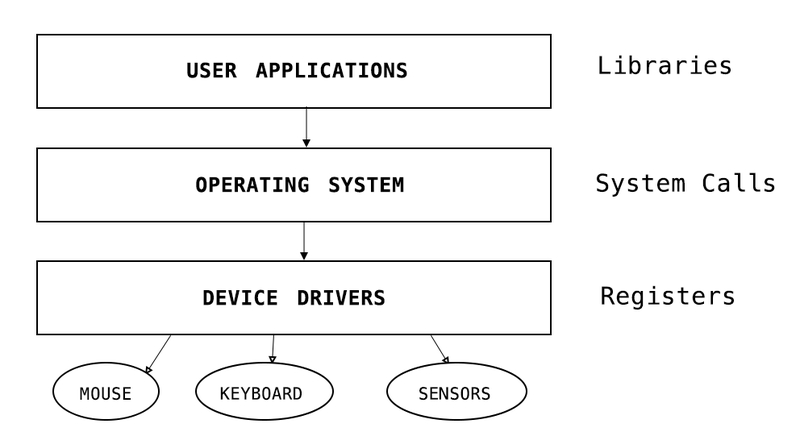
Overview of iteration between device drivers and operating system.
Since the device driver is proprietary and given that it is a “bottleneck” for controlling the hardware, we are very interested in understanding how a device works and what settings it can provide. It is indeed possible to hide features by setting stringent limits via the device driver ― not surprisingly, most problems with peripherals occur because of a problem with the device driver and not the device itself. However, the manufacturer does not always attach the device driver. It is also possible to write it from scratch, following documentation from the manufacturer.
To share data from a peripheral and transmit it to the mainframe, there are two main techniques:
- Programmed Input Output (PIO) ― a technique originated in the early days of computing that continues to be used for embedded devices. Its main purpose is to transfer data between the memory and the peripheral, using the central processing unit (CPU). Interferes with normal execution flow.
- Direct Memory Access (DMA) ― optimization of the Programmed Input Output technique. Provides for a new device that interfaces directly with memory and peripherals, but does not involve CPU contribution.
In the following paragraphs, we will explore the difference between the two techniques by introducing a communication protocol that is used within the Reolink RLC-810A camera.
Programmed Input Output
The Programmed Input Output technique is a method of data transmission between a peripheral device and the CPU. Each data transfer is initiated by an instruction in the program involving the CPU. The processor executes a program that gives it direct control of the I/O operation, including detecting the status of the device, sending a read/write command, and transferring data.
The operation of the Programmed Input Output can be summarized as follows:
- The CPU is executing a program and encounters an instruction related to an I/O operation.
- The CPU executes the instruction, querying the peripheral device.
- The peripheral device performs the requested action according to the instruction given by the CPU and sets the appropriate bits in the status register.
- The processor periodically checks the status of the I/O module until it detects that the operation has not been completed.
As one can easily guess, Step 4 uses the CPU for the longest period of time ― cyclically checking the status of the operation is an unnecessary waste of time. This is the main disadvantage of the Programmed Input Output technique. The CPU must stop the execution flow in order to periodically check the status of the peripheral, which impacts system performance.
The second disadvantage of PIO lies in the size of the data that can be sent to the CPU. Since the registers are fixed and small in size, the CPU must spend several clock cycles in an effort to transfer large masses of data. PIO speeds range from a few kBytes per second up to 55 MB per second, which is more than enough for some embedded purposes.
On the other hand, not implementing a DMA allows for simpler electronic logic. This strongly impacts development costs, making large-scale savings possible. The simplicity of PIO is strongly chosen by embedded device manufacturers because peripheral devices do not need to transfer large amounts of data at high speed. For the connection between the OMNIVISION optical sensor and the board, Novatek decided not to implement DMA, instead taking advantage of one of the two CPU cores that is fully dedicated to image encoding.
Direct Memory Access
When you have multiple hardware devices (e.g., network card, keyboard, mouse) transferring data abruptly, such as in a general-purpose system, the use of the PIO could weigh on CPU performance. Therefore, it is necessary to think of further optimization that can eliminate the CPU’s contribution.
To access registers, both the operating system and devices must share a common space. Using the generic registers already provided by the CPU is out of the question, because it would mean occupying the CPU for some time and essentially stopping the execution of OS processes. The solution lies in adopting a device called DMA (Direct Memory Access) that allows devices to access main memory without querying or interrupting CPU execution flow.
It may not seem intuitive as an approach, but the original question asked was: Where can we store registers? The immediate thought is main memory (i.e., RAM) as a shared space to map registers. The problem, however, is that RAM can only be accessed through the CPU. In fact, the CPU is the only hardware element that can retrieve a piece of information given by a RAM address. By implementing a new method of retrieving data, leaving out the CPU’s contribution, DMA allows devices to access their own registers without having to interrupt the execution flow ― a significant saving in resources and time!
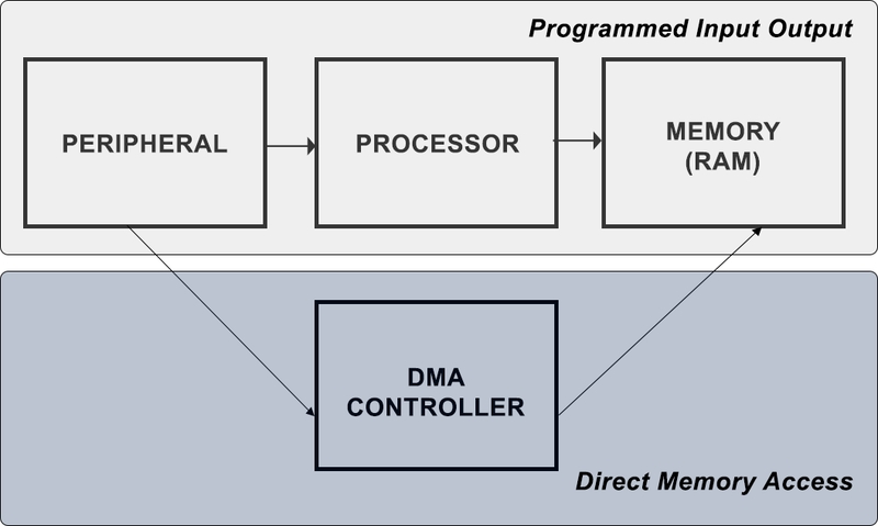
Difference between Programmed I/O and Direct Memory Access.
Since main memory allows the storage of multiple registers, there is currently no “virtual” limit to the number of registers per device. Each device has a set of registers that are mapped to main memory at some specified address. The device driver knows both how to manipulate the registers and address locations. Here, you have very simplified and highly optimized device management.
The DMA, in particular, is concerned with moving data from the bus (communication channel where different signals flow) to the memory and vice versa. The peripheral device does not have to worry about handling the signals to the DMA, but simply places them on the bus.
Bus
How do signals arrive from the peripheral to the DMA controller? Primarily through a communication channel called the bus shared by all peripherals and the mainframe. The bus represents the method by which data is communicated between all parts inside the mainframe.
Within a board, there are mainly three types of buses that are similar to the three types of registers mentioned in some previous paragraphs. These include: the data bus, which allows data to be shared between devices; the address bus, which tells devices the destination of data; and the control bus, which coordinates activity between various peripherals to prevent data collisions. A collision happens when two devices send signals at the same time causing data corruption.
When a peripheral wants to write some data within its own register, it uses a fixed address that allows a controller to map that register within memory. This action can be performed either by a DMA controller or by the CPU itself.
General Purpose Input Output
Another important device within peripheral management is the General Purpose Input Output (GPIO), a generic hardware interface that allows microcontrollers to interact with other devices. From a hardware point of view, it is a series of “general purpose” PINs where each PIN can be freely set to function as an input or as an output.
The GPIO proves essential for bringing power to peripherals that require it, such as in the case of the OMNIVISION optical sensor. Handling the GPIO and the different PINs requires great skill and care, because if you connect a device to the wrong PIN, there is a risk of an electrical current damaging part of the device.
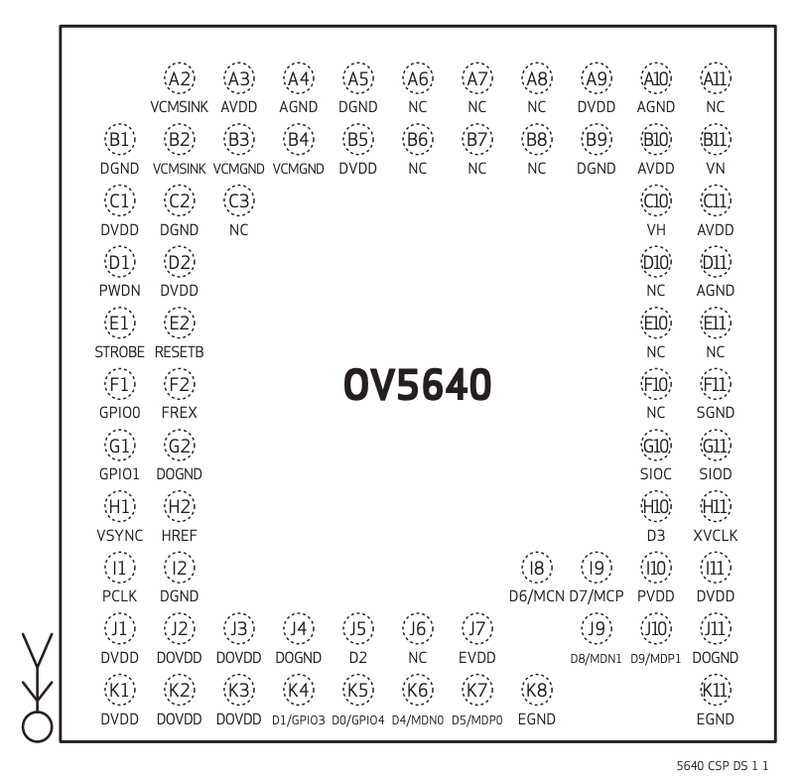
Example pin diagram for an Omnivision sensor
The manufacturer encloses, with the peripheral device, a diagram that allows the different PINs to be connected to the GPIO. The CPU using the different PINs allows the device driver to be able to change state to the peripheral device.
I2C Protocol
Now that we have introduced some theoretical concepts, we can address a bus communication protocol used in Novatek’s board ― the I2C protocol. The I2C protocol is a communication protocol designed to connect integrated circuits that are on the same board.
The bus represents a shared cable through which different information passes. To avoid potential problems (e.g., collisions between various signals), it is necessary to use a protocol ― a set of rules that determines how to send signals and when. Note that I2C does not define the semantics of messages (i.e., how they should be interpreted), only the timing.
The acronym I2C stands for Inter-Integrated Circuit Bus and was primarily introduced by Koninklijke Philips N.V. (a.k.a. Philips) to connect integrated circuits inside 1980s TVs. This led to larger transistors being abandoned in favor of early integrated circuits.
Each device connected within a bus can have two main roles:
- Master ― a device that takes responsibility for the conversation, generates the clock, and initiates communication to slave devices. Only one master can be present for the I2C protocol.
- Slave ― all other devices that respond to requests from the Master receive the clock from the Master.
I2C has two main buses that connect all peripheral devices. Specifically, SDA (Serial Data), bidirectional that allows serial data exchange and SCL (Serial CLock), unidirectional from Master to Slaves that stores the clock for transmission. Typical voltages used are 3.3 V or 5 V.
To identify each device connected to the bus, the protocol uses a 7-bit address system and, additionally, another bit that indicates which operation the Master device is requesting (whether to write 0 or read 1).
Let’s take a look at what happens when a Master requests a write operation on a peripheral:
- Master sends a
STARTsignal identifying the desire to initiate a new connection. - Master sends the address of the peripheral it wants to query.
- Master sends the number of the register to be written.
- Master sends the data that is to be written (note that this point is repeated for each register that is to be written).
- Master sends the
STOPsignal identifying the end of the transmission.
Similarly, for a reading operation:
- Master sends a
STARTsignal. - Master sends the address of the device it wants to query.
- Master sends the number of the register to be read.
- Master sends a new
STARTsignal. - Master sends the address of the device.
- Slave sends data (this step is repeated for each register to be read).
- Master sends the
STOPsignal.
This sequence of signals must be sent for each write and read operation. The I2C protocol also has support for operation with feedback. For each byte written or read, the Slave device responds with an ACK signal (one bit to 0), called an acknowledge, indicating whether the operation was successful.
Depending on the version of the I2C protocol used, this can be as high as a few MB per second, which is more than enough to handle quantities of data on embedded devices. By taking advantage of I2C addressing, it is also possible to connect multiple Slave devices controlled by a single Master.
I2C is employed in a multitude of hardware devices and has now become a de facto standard in driver interfacing. Reolink’s IP camera and all of Novatek’s boards are good examples of this. While I2C technology requires few wires for multiple devices, it also presents some problems that should not be overlooked during design. These include the data exchange speed, which is very slow because at least seven messages are required to exchange one byte of data. I2C presents a complex logic to implement, because of its feature of associating an address with each device. Therefore, it may not be the best choice for devices with extremely limited resources.
UART
UART is the second communication protocol that this article seeks to explore. UART stands for Universal Asynchronous Receiver-Transmitter, an asynchronous serial communication protocol in which the data format and transmission rates are configurable. It sends data bits one by one, from least significant to most significant, framed by start and stop bits so that the precise timing is handled by the communication channel.
For UART to work, the settings must be the same on both the transmitting and receiving sides. UART can be configured with:
- Baud rate ― pulses per second, this is the number of changes from 0 to 1 per second;
- Parity bit ― used to check for errors;
- Data bit size;
- Label to recognize end of data ― character that is added to the bottom of the data frame to identify the end of the data to be sent; and
- Data for flow control ― a set of commands to set UART.
The speed that UART provides is very similar to the speed provided by an I2C interface and operates very similarly to the I2C interface. The UART protocol can operate in three different ways:
- Simplex ― data is conveyed in a single direction: from source A to receiver B;
- Half-duplex ― data can be sent from both A and B, however, data cannot be sent simultaneously; and
- Full-duplex ― data can be sent from both A and B and data can be sent simultaneously.
Unlike the I2C protocol, the UART protocol has no reference clock, so it cannot rely on the concept of time to know when to start reading bits. Therefore, when the UART receives a start bit, it will start reading bits at the rate defined by baud rate. It is therefore crucial that receiver and source adopt the same configuration or else data will be lost.
Better Methods
There is no absolutely best method of communication between the motherboard and input/output devices. In fact, from case to case, the manufacturer can choose whether to get more speed at the cost of resources, or vice versa, save for less data.
Now that we have delved into all the sections for interfacing with the hardware and acknowledged the possible drawbacks of each technology, we can move on to analyze a driver contained in the lib folder. See you next Wednesday for more analysis of a driver that uses the I2C protocol!
Reolink Serie
- Part 1 – Introduction to Firmware Analysis of a Reolink IP Camera
- Part 2 – Booting an Embedded OS: the Booting and U-Boot Phase
- Part 3 – Dissecting Reolink RLC-810A Hardware: A Detailed View
- Part 4 – Understanding the UBI File System in Embedded Devices
- Part 5 – Exploring the Operating System of Reolink RLC-810A
- Part 6 – Techniques for Setting up Peripherals via PIO and DMA
- Part 7 – Reverse Engineering the OMNIVISION OS12D40 Driver