Dissecting Reolink RLC-810A Hardware: A Detailed View
Published at – 17 min read – 3558 words
Now that we know how device booting works, let’s try to extract some parts from the firmware that we downloaded in Part 1 of our series. Here, we are interested in two main sections: the Linux kernel (which takes care of booting the device services) and the flattened device tree (which allows the kernel to know the hardware configuration a priori without inspecting each device).
During the course of this article, we will also proceed as hardware manufacturers and, with a critical eye, comment on each choice made by the manufacturer.
Extracting Image with dd
To begin, we will try to do a manual extraction using the dd tool and the result obtained from an analysis with Binwalk. From there, we will use the tools already provided with Binwalk.
The dd tool is part of a set of utilities already provided on Linux for copying the contents of a file verbatim by specifying the offset. dd can duplicate data from files, various devices, partitions, and volumes. Its syntax is simple enough to understand:
dd if=input_file of=output_file bs=1 skip=offset count=how_many_blocks
We identify which of the parts from the previous result we want to use. Specifically, we want both the flattened device tree and the initial Linux executable:
34600         0x8728          Flattened device tree, size: 17375 bytes, version: 17
624319        0x986BF         uImage header, header size: 64 bytes, header CRC: 0x7B9F6E31, created: 2021-06-19 06:29:15, image size: 3153472 bytes, Data Address: 0x8000, Entry Point: 0x8000, data CRC: 0xD7FC213, OS: Linux, CPU: ARM, image type: OS Kernel Image, compression type: none, image name: "Linux-4.19.91"
Let’s remember what data we are interested in: the offset (at the beginning of the line) and the size of the file we are going to extract (image size). We also specify the unit of measurement (i.e. 1 byte bs=1). The command to extract the kernel image will be:
dd if=firmware_rlc_810_a.pak of=linux_image bs=1 skip=624319 count=3153472
Another simple command (file linux_image) will show confirmation of the extraction:
linux_image: u-boot legacy uImage, Linux-4.19.91, Linux/ARM, OS Kernel Image (Not compressed), 3153472 bytes, Sat Jun 19 06:29:15 2021, Load Address: 0X008000, Entry Point: 0X008000, Header CRC: 0X7B9F6E31, Data CRC: 0XD7FC213
Whereas, the one for the flattened device tree is:
dd if=firmware_rlc_810_a.pak of=device_tree bs=1 skip=34600 count=17375
Again, the file device_tree confirms successful extraction:
device_tree: Device Tree Blob version 17, size=17375, boot CPU=0, string block size=1495, DT structure block size=15824
A careful reader might wonder whether it was worthwhile to tackle this manual analysis section instead of running Binwalk. It turns out, however, that manual analysis is exactly what Binwalk does. Simply put, it analyzes the raw bytes and if it finds a match with a particular signature, it tries to unpack the header file. If the data is valid, then it tries to extract the image from the analyzed file.
Flattened Device Tree of Reolink
Before continuing with the more serious analysis using Binwalk, it is useful to explain the flattened device tree file format, which allows the operating system to know in advance the hardware devices that are present within the embedded system.
In general-purpose environments, when the operating system is loaded into memory, it proceeds to inspect all connected devices to populate a table indicating the information of each device. For example, what should the operating system do when the keyboard is running? Or when the mouse is moving?
In order to match a real action to a virtual (input) event, the operating system tracks all devices so that it knows how to handle any event from the hardware devices. It must also know how to transfer virtual events into physical actions for output. In order to avoid having to query every single hardware device every time at start-up, we can take two approaches: one is to write the individual devices to be loaded directly into the code and the other is to read the various configurations from a file in the file system. Both approaches do not seem to be the right way: the former inevitably suffers from problems (How can we dynamically configure a device?) while the latter may be slow (the operating system should at least know the device to read from).
The solution lies somewhere in between the two approaches seen in the previous paragraph: the flattened device tree, a section specifying the board’s set of devices. This section is loaded immediately at boot time and allows the operating system to understand which drivers to load and which not to load. The operating system only needs to check the status of the devices, instead of inspecting each hardware controller.
We then proceed to analyze the flattened device tree. Once extracted, we can view its contents using a tool called the device-tree-compiler. From there, we install the package and proceed to explore the ReoLink camera hardware:
dtc -I dtb -O dts -o - device_tree
The flags specify what file format to use ― in input DTB (Device Tree Blob) and in output DTS (Device Tree Source). A very useful guide to the device-tree-compiler can be found at git.kernel.org. The complete file can instead be found at Github.
So let’s begin by inspecting the hardware of the Reolink RLC-810A IP camera. What follows is a fairly technical overview, as it would take many articles to fully explain each device in detail. I suggest that you dwell and delve into what you are interested in.
Each device tree starts with some specification of the type of board or system-on-a-chip used. These files are produced by the manufacturer of the board on which the system is built, so they can be useful to understand what kind of hardware has been placed inside the product.
model = "Novatek NA51055";
compatible = "novatek,na51055\0nvt,ca9";
The model field reports a rather popular Taiwanese company named Novatek Microelectronics Corp that designs and manufactures integrated circuits. The board is called NA51055 and appears to be a variant of the more commercially known NT9852x model. Through a Google search, the board seems to have been used not only for Reolink, but also for some dashcams of the company Viofo. It is indeed not uncommon for one type of board to be used by more than one company, since many embedded devices are similar in functionality (whether it be a dashcam or camera, it only changes what to record).
After this brief specification, all hardware devices on the board are summarized. Each device follows a precise pattern; although, not all parameters are always specified:
device_name {
	reg = // registers value
	interrupts = // interrupts to which the device responds
	compatible = // string allowing the kernel to identify the device driver capable of handling the device
	clock = // reference to the clock used by the device
}
One more note on the compatible property: the operating system uses this property to know which device driver to connect the device to. To find out more information about the type of driver and how it communicates with this device, we need to reverse engineer a driver.
Reolink Hardware
We proceed to highlight some hardware devices:
CPU ― data processing device. For this board, an ARM Cortex A9-based CPU was used, maximum clock frequency around 1GHz. The CPU is very similar in power and capability to the CPU mounted on the iPhone 4S.
Cache ― model
pl310: hardware controller that manages the data/instruction cache (it sits between the RAM memory and the CPU). It speeds up execution by not having to keep fetching instructions from RAM (very expensive).UART devices ― convert data from a parallel format to an asynchronous serial format or vice versa.
MMC ― hardware controller for reading/writing to microSD devices.
NAND ― flash memory inside the board, usually where the operating system is installed; interestingly, within the flattened device tree, all the partitions of our system are also specified. It is therefore possible to specifically try to find out how the image is composed when the operating system boots.
Encoder JPEG ― component that natively encodes data streams from the optical sensor into JPEG frames to construct an image stream.
Another set of low-level hardware devices such as Watchdog, analogue-to-digital converter, real-time clock, etc.
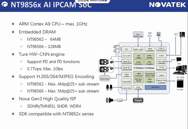
Elements located within the SoC and their functions. Source: ambchina.com
CPU
The CPU is the main hardware element to be studied within a board. The job of a CPU is to process information. It takes the instructions from the memory that are to be executed, executes them, and places the result in some registers. In fact, each CPU has associated memories that are very small in size, but at the same time are very fast to write or read ― these memories are called registers.
As confirmed during Part 2 of our series, the architecture of the Reolink camera is the typical Advanced RISC Machine (ARM) architecture that we can find in any other embedded device. The architecture of a computer defines the type of instructions (i.e., what the CPU has to process) and how the CPU computes these instructions. The ARM architecture is among the most widely used for embedded devices due to its low power consumption compared to other architectures.
Which devices are based on the ARM architecture? To name a few: Nintendo DS, Nintendo DSI, iPhone 3GS, iPod, etc. As main features, we find a 32-bit register set, fixed-length instructions to simplify decoding and execution, RISC instructions.
It is good to do a little background on the RISC concept. RISC stands for Reduced Instruction Set Computer and indicates an architecture design idea that favors the development of a simple, linear architecture. To execute any kind of program, the CPU processes/computes instructions (e.g., take this data from memory and do an addition). The instructions that a CPU processes are very close to the hardware, as there is a direct connection between the choices in hardware design and the complexity of the instructions.
With more complex instructions, the CPU allows for less complex and shorter code, because the device abstracts some concepts and makes a less complex interface available. On the other hand, however, to increase the time needed to complete an instruction, one would decrease the speed. Another choice could be less complex instructions ― a code of greater length, less complexity, but increased speed.
To explain this even further, let’s introduce a particular device called the clock, which ensures perfect synchronization between all the components inside the CPU. The clock is very similar to a metronome and gives the CPU time. A clock cycle is the minimum time unit for which instruction processing is measured. If you have a 1GHz CPU, this means that the frequency of the clock cycle is 1GHz and therefore about 1 billion instructions every second, assuming one clock cycle = one instruction.
The clock is an arbitrary tool ― any designer can increase or decrease the speed at which the clock gives the signal to the CPU. Of course, it is a very balanced process: if the clock is too fast, there is the risk of the CPU losing instructions, if the clock is too slow, there is the risk of the CPU wasting unnecessary time. Since we can decide how fast the CPU processes these instructions, less complex instructions seems to be the ideal approach compared to “fewer, more complex instructions”. Increasing speed by decreasing instruction complexity is very simple: just increase the clock speed! It is more difficult, however, to increase speed with instructions that are intricately more complex. A higher clock frequency in the latter case would not benefit the machine, as it would run the risk of skipping instructions.
The approach of “more instructions to execute, less complex” is the approach chosen for RISC architecture and allows more limited energy consumption (less complexity, less current used). This characteristic makes RISC and ARM the preferred architecture for most embedded devices.
Introduced in 2007, the typical ARM Cortex-type CPU has some of the following features:
- L2 cache controller up to 4MB: the controller for the level 2 cache;
- 8-stage pipeline;
- Multicore processing;
- Thumb-2 as instruction set encoding that reduces program size; and
- MMU enabled: Memory Management Unit, an internal CPU component that enables virtual memory support.
In particular, we note that Novatek’s board has a 2-core CPU. This is very important, because it actually allows two programs to run in parallel. According to some research, and the fact that we found some strings that can be traced back to RTOS, it is possible that one CPU runs the IP camera core (capturing the image and transferring it to a continuous video), while the other runs a custom Linux-based distribution. For now, we do not worry too much about the real-time part. It is enough to know that there is a graphics engine that takes care of saving the images captured by the optical sensor.
Our investigation of the CPU unfortunately ends here, as we have no further information from Novatek. A document showing the datasheet of the NT96650BG board can give you an idea as to the degree of secrecy Novatek assumes with respect to their information.
NAND memory
NAND flash memory is used as space for the operating system and application files (binaries that control the camera, configuration files, etc.). It is normally soldered onto the board and once content has been written to it, rewriting or re-flashing requires some extra care.
This type of memory is a very large category of storage media (solid-state disk) that stores data through a configuration of transistors. These transistors (which may represent NOR or NAND ports, depending on the case) retain an electrical charge for a long time. Each transistor constitutes a memory cell that stores the value of a bit ― having several memory cells in series or in parallel makes it possible to store tons of data.
Let’s not get into the intricacies of the hardware, but we can see a posteriori how the FP2024 5F1GQ4UBYIG memory produced by GigaDevice is used.
It is interesting to see how a priori we can predict the layout of the NAND flash, by browsing the NAND section of the flattened device tree embedded within the kernel. In particular, we can find within the flattened device tree:
- Loader partition ― component in charge of loading the operating system, memory area
0x0of size0x40000. - Partition FDT (file
nvt-na51055-evb.bin) ― the flattened device tree, loaded into the0x40000memory area of size0x40000. - Partition fdt_restore ― contains a copy of the flattened device tree to be used in case of unexpected failure, loaded into the
0x80000memory area of size0x40000. - U-Boot partition (file
u-boot.bin) ― contains the U-Boot bootloader, size0x18000starting at0xc0000. - uEnv partition ― contains the boot parameters for U-Boot, size
0x40000starting at0x240000. - Kernel partition (file
uImage.bin) ― contains the Linux kernel image (initrd), size0x480000starting at0x28000. - rootfs partition (
rootfs.ubifs.binfile) ― contains the file system image with configuration files and the operating system, size0x2000000starting at0x700000. - appfs partition (
appfs.ubifs.binfile) ― contains the set of application-specific files, size0x1500000starting at0x2700000. - Other free partitions used for installing new firmware from the web interface.
Double-checking the available NAND memory during boot: 0x80000000 ➔ 134217728 bytes ➔ 128 Mebibytes (MiB) ➔ 220 Bytes. So, we find a match between NA51055 (probably designed for ReoLink) and NT98523 (mentioned in the flattened device tree).
Board Hardware
However, I found discrepancies between the Novatek models mentioned within the firmware and what was physically used inside Reolink. To confirm the hardware part and investigate the firmware further, we can check the internal images filed with the Federal Communications Commission (FCC). However, let’s take a step back to better explain the role of the FCC.
When any manufacturer wants to market a product in a certain country, it must comply with certain laws that regulate the use of frequencies and the impact it has on frequencies already in use. For the United States, the regulatory body that verifies each product and certifies its safety is the FCC. The commission has its own mark that certifies that the electromagnetic interference from the device complies with appropriate limits.
Every manufacturer selling a product in the United States must certify electromagnetic safety by making arrangements with third-party laboratories to perform certain tests and measurements. If the commission approves the data for a certain product, then the manufacturer receives the FCC mark and the device can be offered for sale.
In the interests of transparency, all applications are publicly visible and anyone can view the test results ― including the internal pictures of the product. Since I do not have a Reolink product, I preferred to consult and inspect the images already available in the FCC archive. FCCID allows one to explore all applications received by the FCC. Just type in Reolink to access the certifications from Reolink Innovation Limited, the company that owns the hardware produced.
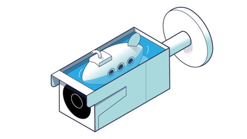
We are interested in the report for the product 2AYHE-2012A. The Reolink RLC-810A is an identical copy of the Reolink RLC-511WA, with the only difference being the optical sensor. As we can see from the internal photos, Reolink RLC-810A mounts the NT98523MBG 2004-BB T8N60400 processor. For the internal flash memory, a 128MB card from GigaDevice (FP2024 5F1GQ4UBYIG) is confirmed, as we expected from the flattened device tree. The device is also equipped with 256MB RAM from SKHynix (H5TQ2G63GFR-RDC 025A NWMN9528HF).
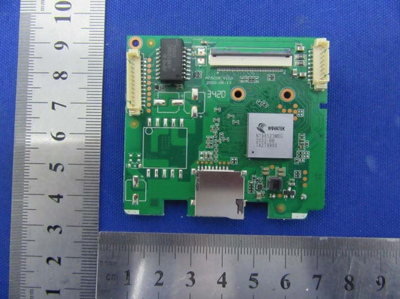
NT98632MBG processor - internal image from FCC report
The internal layout is almost identical to the RLC-511WA, because it has the same features as the RLC-810A ― only for one small difference, namely the optical sensor. Various reports (such as TechInsights and forum mobile01.com) show that Reolink has chosen the O12D40 sensor from the company OMNIVISION for the RLC-810A, which allows video to be stored up to a maximum resolution of 4512x2512. This, however, stands out somewhat from the specifications presented by the manufacturer, which show a maximum resolution of 3840x2160 with a maximum of 8 MP. In all likelihood, the company preferred to keep the resolution lower than the maximum because of the less powerful CPU, as opposed to the one that would be needed to process higher resolution videos.
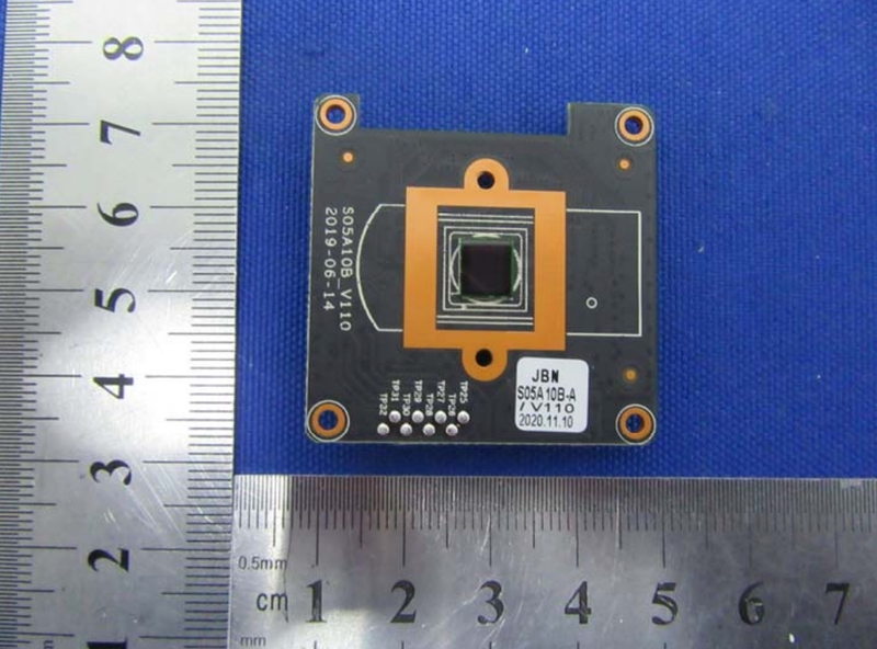
The 5MP sensor used by the Reolink RLC-511WA 'twin' model - internal image from the FCC report.
Reolink therefore used the same memory layout with the same power, but attempted to achieve greater definition with a different optical sensor. This technical “miracle” is made possible by a powerful firmware that manages to minimize the load on the CPU. This miracle, however, has some limitations and flaws. In fact, there are many reviews reporting that the viewing and recording of 4k movies is unstable. We will explore this problem in more detail in subsequent articles.
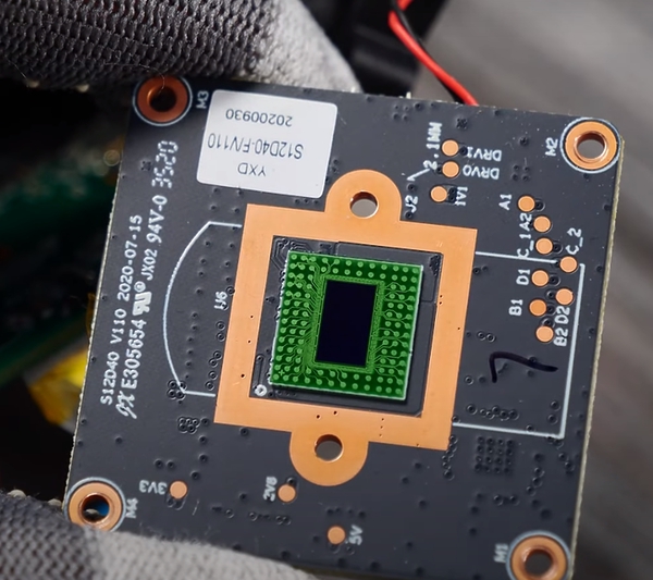
The sensor used by RLC-810-A, OS12D40-PB-v1.1.0
Conclusion: Centralized Hardware
It is not the task of this series to delve further into all hardware devices, so the hardware section ends here. In summary, let’s end this article with a couple of thoughts. I am not a hardware expert, so take everything in this article with a grain of salt.
We have realized how complex a device can be both from a technical and a “logistical” point of view ― between RAM, CPU, cache, etc., there is not just one supplier but several companies that contribute to the development of the board. We have also seen how the companies (Reolink and many others) share the same hardware (with different pricing) bought from the same manufacturer (Novatek). Therefore, there is a risk that hardware is centralized and a problem on one board may be common across many devices.
Another reflection on hardware concerns security by obscurity, a practice that relies on secrecy in the design or implementation of a system. In this case, the “secrecy” of the system lies in the device, which cannot be easily inspected visually because the integrated hardware/circuitry is very small. We will discuss “software” secrecy in later articles.
Although the Reolink device has been tested and certified, there is no way to verify every hardware element from a security point of view. Furthermore, not much information can be obtained from open sources ― probably to protect the company’s intellectual property. Thus, the whole issue of open-source that could benefit the company is missing from Reolink. We hypothesize that this is also partly due to the secrecy imposed by the manufacturer, Novatek.
Lack of transparency can make a difference when cameras are deployed in fairly critical locations ― banks, airports, government offices, etc. Recent articles accuse another company (Hikvision), that produces IP cameras, of being close to the Chinese government. It is certainly difficult to separate what is reality from fantasy (political/ideological conspiracies). What we can only do, however, is to take an objective view of the device and try, via reverse engineering tools, to perform tests/analysis.
Well, this wraps up the third part of this series. See you next week for our fourth installment about UbiFS!
Reolink Serie
- Part 1 – Introduction to Firmware Analysis of a Reolink IP Camera
- Part 2 – Booting an Embedded OS: the Booting and U-Boot Phase
- Part 3 – Dissecting Reolink RLC-810A Hardware: A Detailed View
- Part 4 – Understanding the UBI File System in Embedded Devices
- Part 5 – Exploring the Operating System of Reolink RLC-810A
- Part 6 – Techniques for Setting up Peripherals via PIO and DMA
- Part 7 – Reverse Engineering the OMNIVISION OS12D40 Driver